
Layout view of a simple CMOS Operational Amplifier (inputs are to the left and the compensation capacitor is to the right). The metal layer is coloured blue, green and brown are N- and P-doped Si, the polysilicon is red and vias are crosses.
Digital IC design is to produce components such as microprocessors, FPGAs, memories (RAM, ROM, and flash) and digital ASICs. Digital design focuses on logical correctness, maximizing circuit density, and placing circuits so that clock and timing signals are routed efficiently.
Modern ICs are enormously complicated. A large chip, as of 2009 has close to 1 billion transistors. The rules for what can and cannot be manufactured are also extremely complex. An IC process as of 2006 may well have more than 600 rules. Furthermore, since the manufacturing process itself is not completely predictable, designers must account for its statistical nature.
DESIGN STEPS
A typical IC design cycle involves several steps:
- Feasibility study and die size estimate
- Function analysis
- Layout review
- Design For Test and Automatic test pattern generation
- Design for manufacturability (IC)
- Tape-in
- Mask data preparation
- Tape-out
- Wafer fabrication
- Die test
- Packaging
- Post silicon validation and integration
- Device characterization
- Tweak (if necessary)
- Datasheet generation Portable Document Format
- Ramp up
- Production
- Yield Analysis / Warranty Analysis Reliability (semiconductor)
- Failure analysis on any returns
- Plan for next generation chip using production information if possible
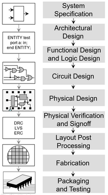
Major Steps in the IC design flow
DIGITAL DESIGN
Roughly speaking, digital IC design can be divided into three parts.
- Electronic system-level design: This step creates the user functional specification. The user may use a variety of languages and tools to create this description. Examples include a C/C++ model, SystemC, SystemVerilog Transaction Level Models, Simulink and MATLAB.
- RTL design: This step converts the user specification (what the user wants the chip to do) into a register transfer level (RTL) description. The RTL describes the exact behavior of the digital circuits on the chip, as well as the interconnections to inputs and outputs.
- Physical design: This step takes the RTL, and a library of available logic gates, and creates a chip design. This involves figuring out which gates to use, defining places for them, and wiring them together.
Note that the second step, RTL design, is responsible for the chip doing the right thing. The third step, physical design, does not affect the functionality at all (if done correctly) but determines how fast the chip operates and how much it costs.
No comments:
Post a Comment